


Effect of folded contact between electrode and dielectric layer on the performance of piezoelectric flexible electronic skin
-
摘要: 提出了一种基于压电效应制备柔性电子皮肤的简单方法。为了研究纳米改性对柔性电子皮肤各层性能的影响,首先以纳米SiO2粒子作为改性体,以聚二甲基硅氧烷(PDMS)作为基体,制备出SiO2/PDMS复合柔性衬底,解决了在PDMS上磁控溅射沉积电极材料产生裂纹的现象,成功获得能够稳定工作的柔性电极。然后用钛酸钡/碳纳米管/聚二甲基硅氧烷(BaTiO3/CNTs/PDMS)复合材料作为功能层,制备出一种五层结构的高灵敏性柔性电子皮肤,并找到一种通过改变基板粗糙度的简单方法构建电极与介电层的褶皱接触,进而提升柔性电极的电导率与柔性电子皮肤的压电响应信号。Abstract: A simple method for fabricating flexible electronic skin based on piezoelectric effect was presented. In order to study the effect of nano modification on the performance of flexible electronic skin, SiO2/polydimethylsiloxane (PDMS) composite flexible substrate was prepared by using nano-SiO2 particles as modifiers and PDMS as matrix. The flexible and stable electrodes were prepared and the crack problem of electrode material on flexible PDMS substrate by magnetron sputtering was successfully solved. The functional layer of barium titanium trioxide/carbon nanotubes/PDMS (BaTiO3/CNTs/PDMS) was implanted in the five-layer structure of the flexible electronic skin that was designed based on the piezoelectric effect. A simple method by varying the substrate roughness was proposed to make a folded contact between the electrode and the dielectric layer. This method improves the conductivity and piezoelectric response of the prepared flexible electronic skin.
-
Key words:
- magnetron sputtering /
- nano-SiO2 /
- flexible electronic skin /
- piezoelectric response /
- flexible sensor
-
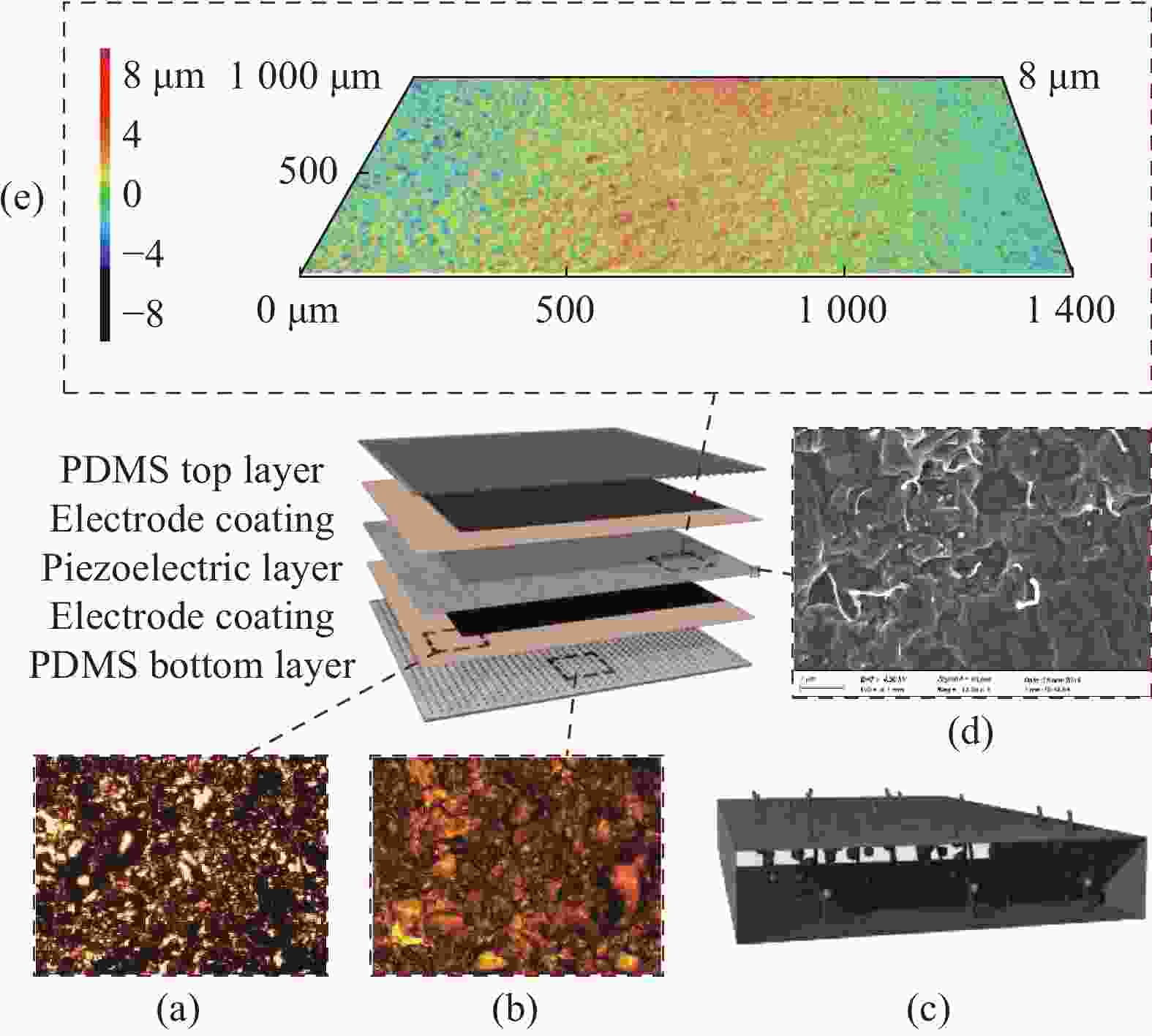
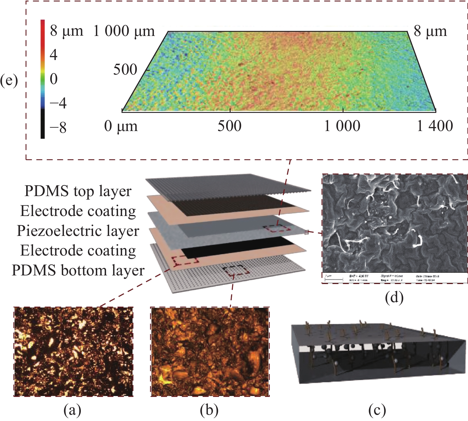
图 1 高灵敏度柔性电子皮肤结构示意图((a)褶皱电极在光学显微镜下单位面积(1 148 μm×856 μm);(b)粗糙聚二甲基硅氧烷(PDMS)在光学显微镜下单位面积(1 148 μm×856 μm);(c)介电层中BaTiO3与碳纳米管(CNTs)分布示意图;(d)扫描电镜下介电层表层形貌;(e)激光显微镜下介电层粗糙表面三维图像)
Figure 1. Layered structure of high sensitivity flexible electronic skin ((a) Foldable electrode images of the thin film per unit area (1 148 μm×856 μm) under light microscope; (b) Rough polydimethylsiloxane (PDMS) images of the thin film per unit area (1 148 μm ×856 μm) under light microscope; (c) Distribution diagram of BaTiO3 and carbon nanotubes (CNTs) in dielectric layer; (d) Surface morphology of dielectric layer under scanning electron microscope; (e)Three-dimensional image of rough surface of dielectric layer under laser microscope)
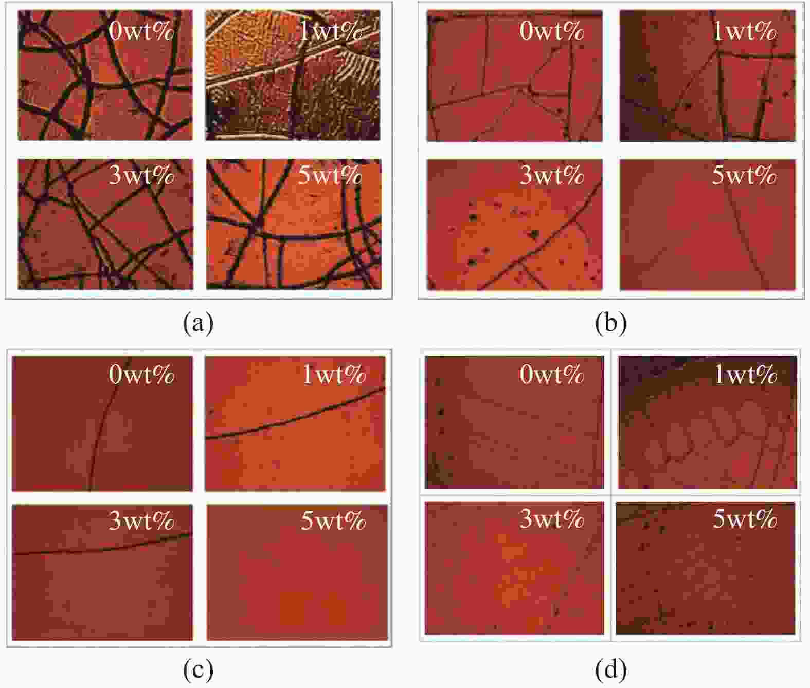
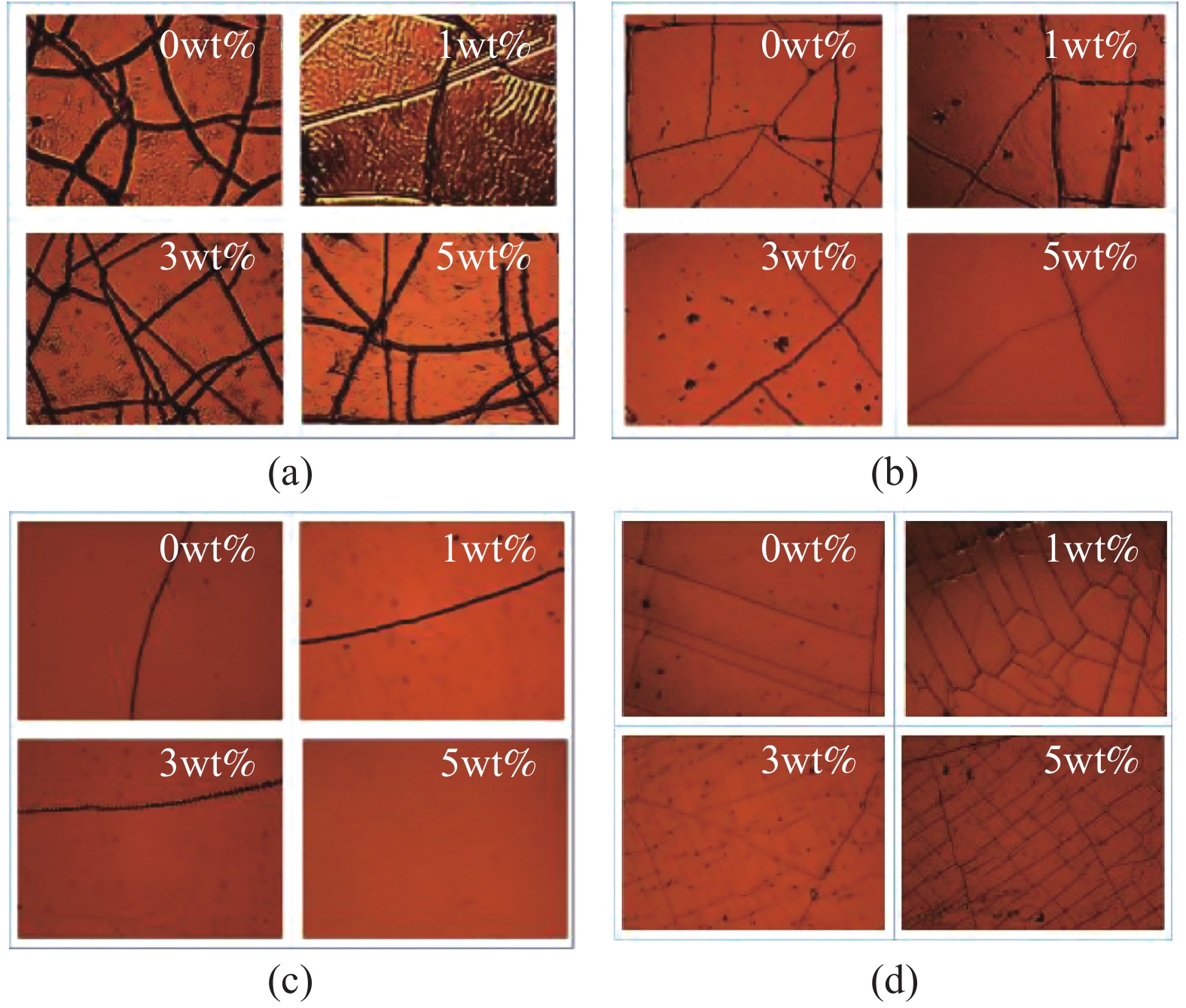
图 4 分别在120 W、100 W、80 W、60 W功率下溅射沉积在PDMS上的铜薄膜在光学显微镜下单位面积(1 148 μm × 856 μm)的裂纹情况(图片右上角标注的是PDMS衬底中纳米SiO2的质量分数,(a)、(b)、(c)载物台为硅片,(d)载物台为Cu片)
Figure 4. Crack images of the copper thin film on PDMS per unit area (1 148 μm × 856 μm) under light microscope, respectively, for the magnetron sputtering power of 120 W, 100 W, 80 W and 60 W (At the top right of the picture is the mass fraction of nano SiO2 in PDMS substrate, (a), (b), (c) silicon platform, and (d) Cu platform)
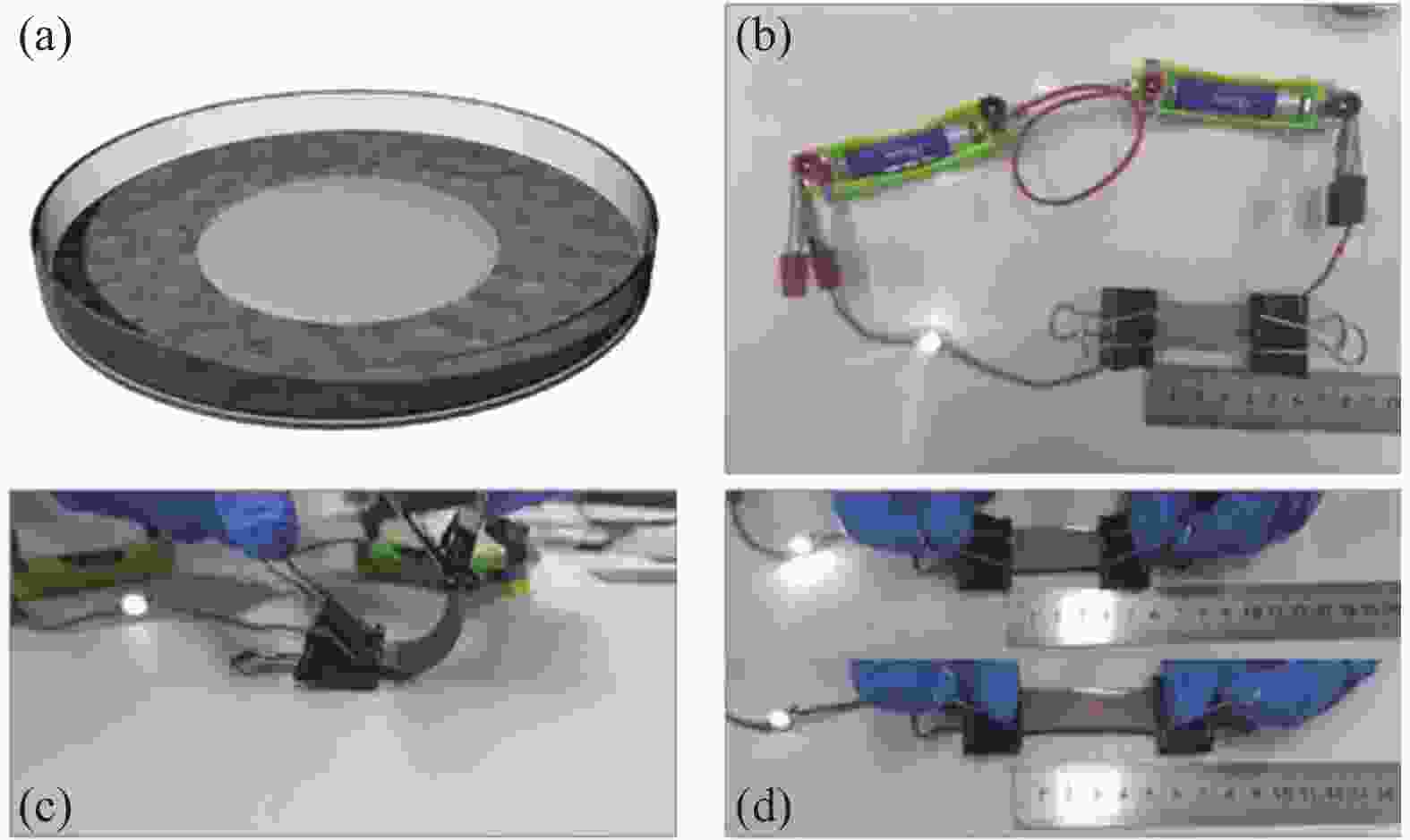
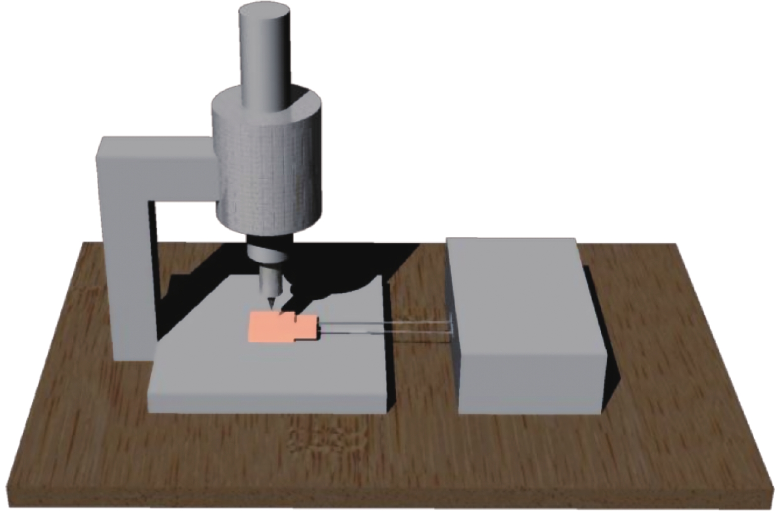
图 5 利用磨砂玻璃制备柔性衬底示意图(a)、测试电路示意图(b)、柔性电极弯曲稳定性检测(c)和柔性电极拉伸检测(d)
Figure 5. Schematic diagram of a flexible substrate prepared from frosted glass (a),test circuit diagram (b), bend stability test of flexible electrode (c) and tension test of flexible electrode (d)
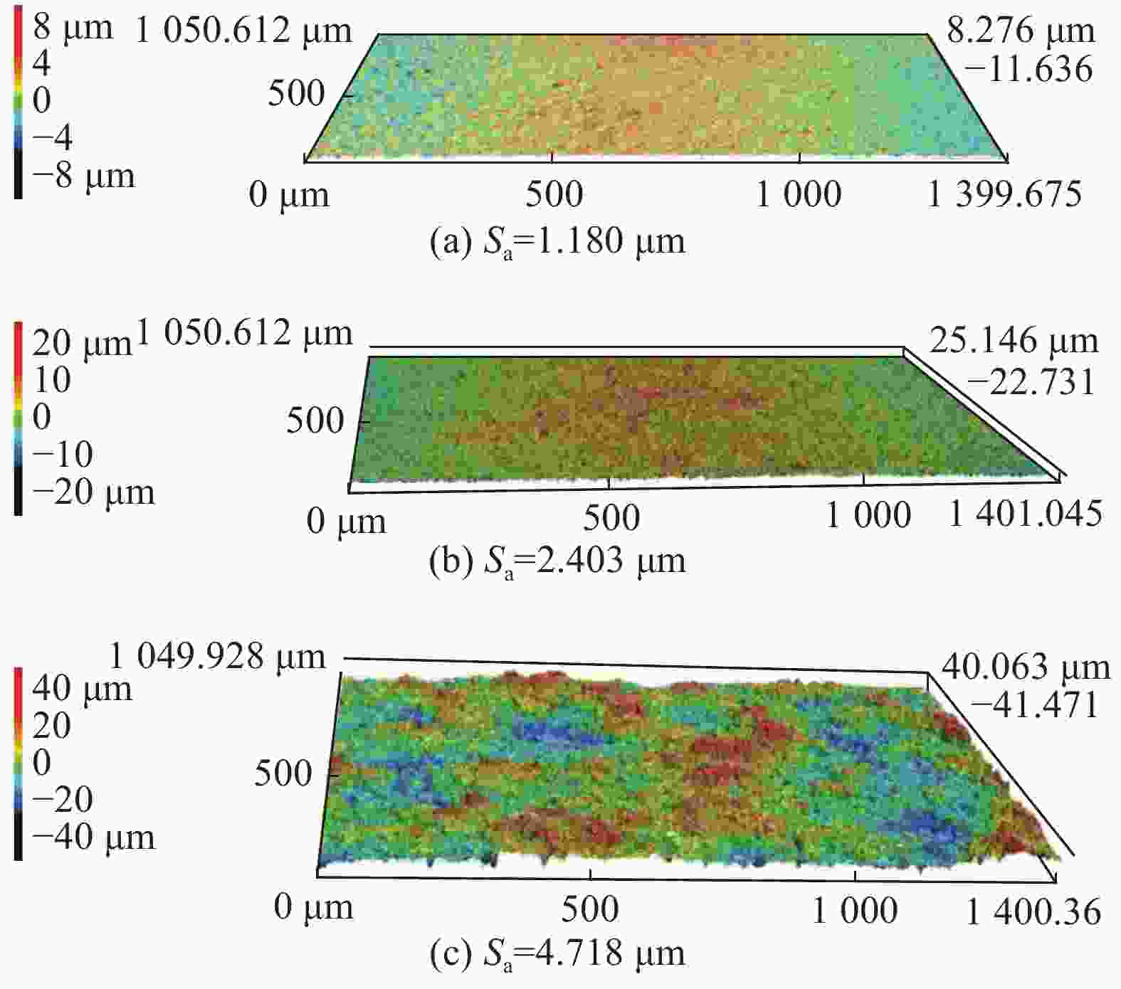
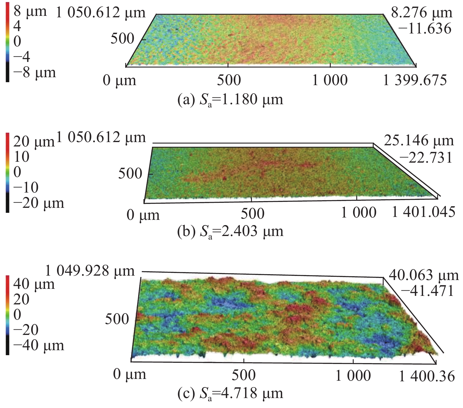
图 6 轮廓测量仪下不同粗糙度介电层的表面形貌
Figure 6. Surface topography of the dielectric layeron with different roughness values under profilometer
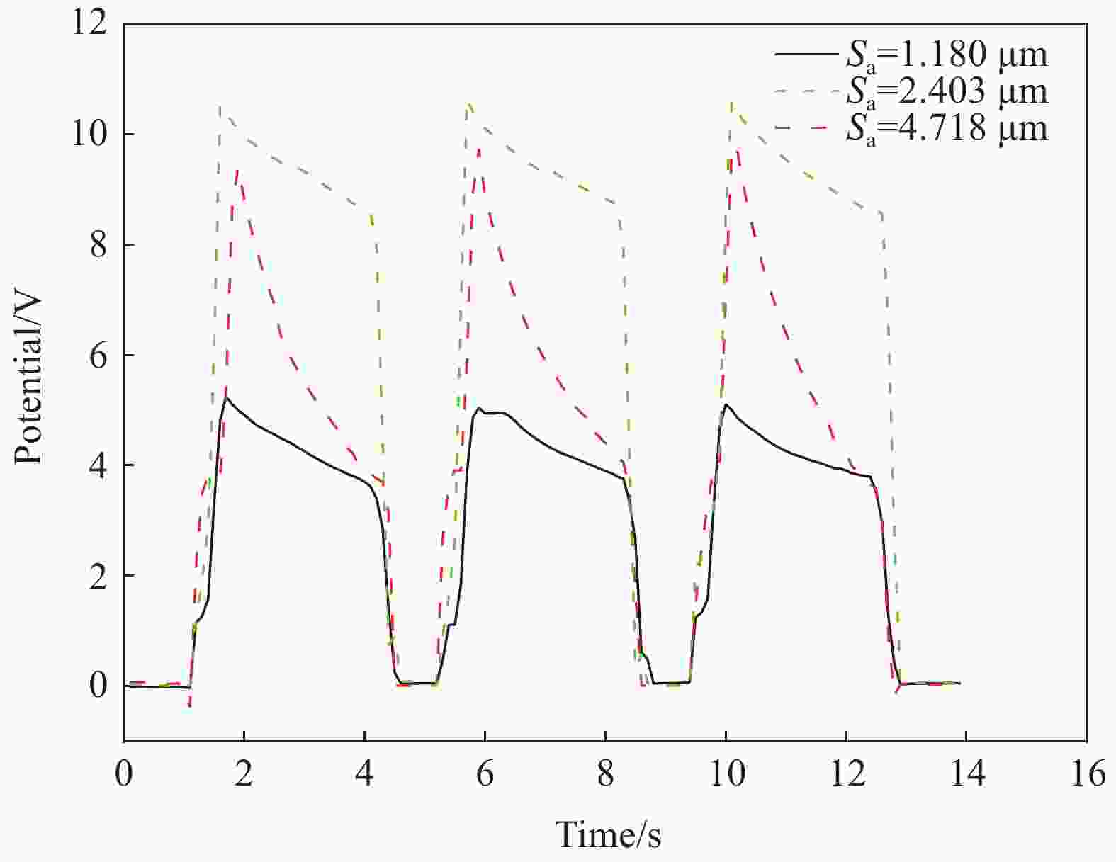
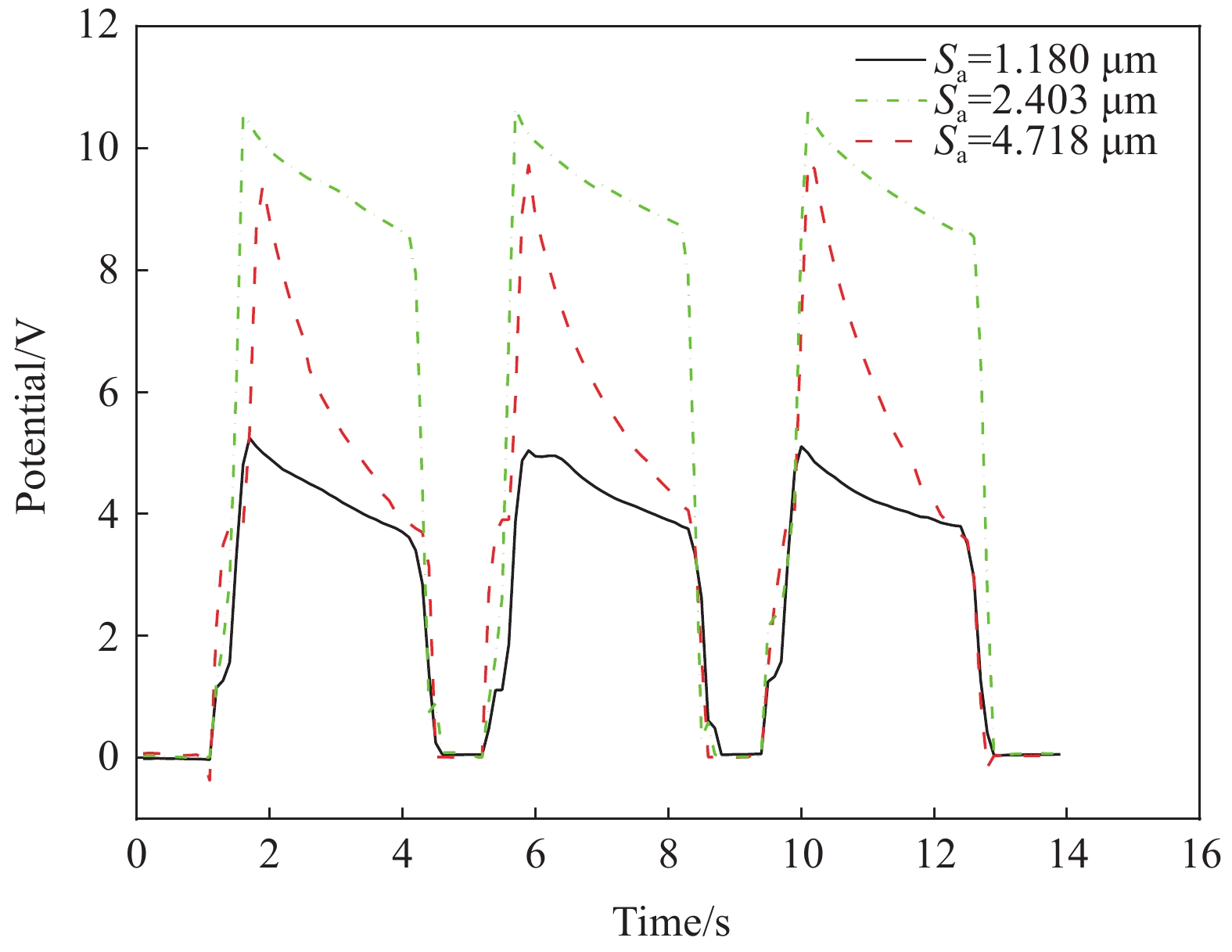
图 7 介电层与电极间不同粗糙度的柔性电子器件的时间-压电信号
Figure 7. Time-piezoelectric signal curves of different roughness between flexible electronic skin electrode and dielectric layer
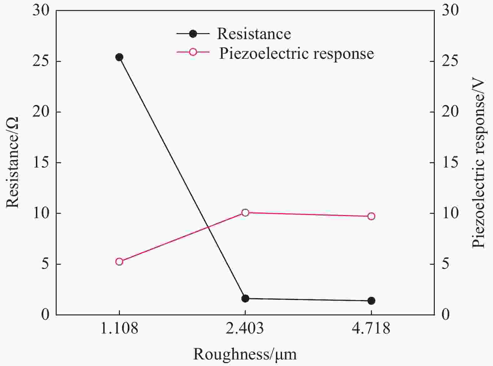
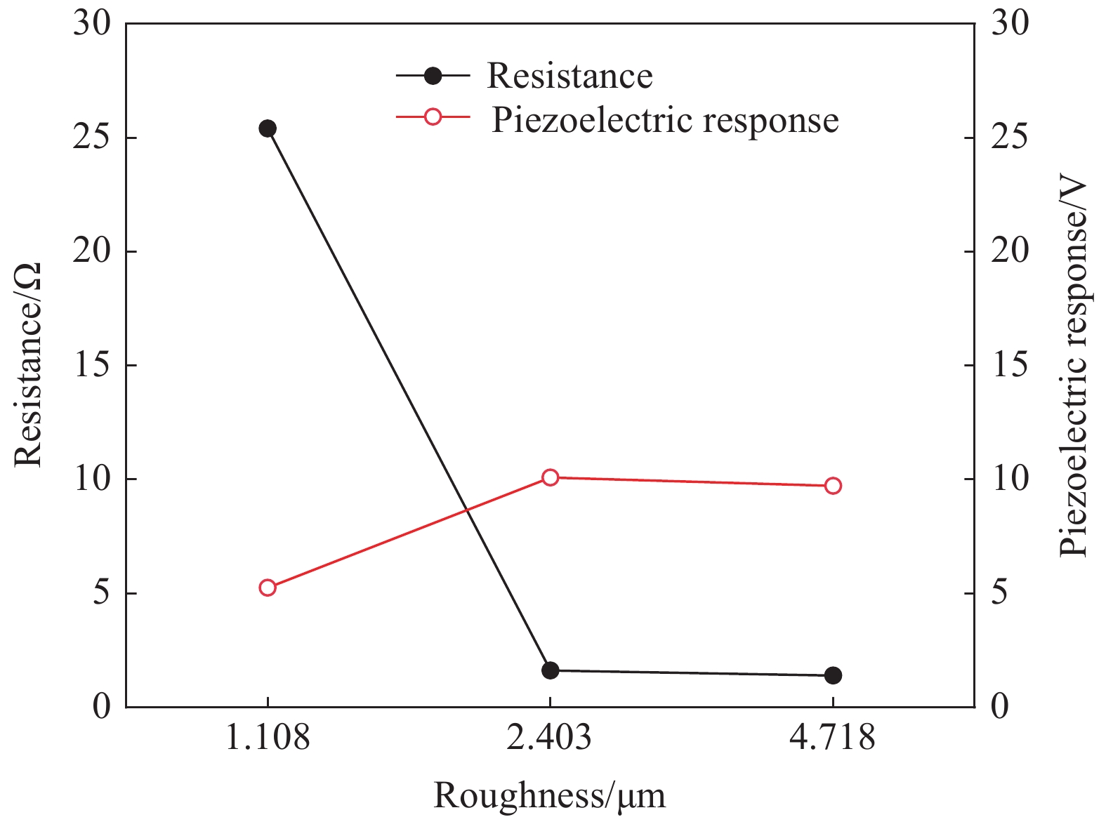
图 8 柔性电子皮肤介电层与电极间粗糙度对电阻率与最大压电响应的影响
Figure 8. Effect of roughness between dielectric layer of flexible electronic skin and electrode on resistivity and maximum piezoelectric response
表 1 介电层实验材料及比例
Table 1. Dielectric layer experimental material and proportion
Material Quality/g Source of materials PDMS 10.0 Dow corning BaTiO3 6.0 Aladdin CNTs/C2H6O 0.5 Aladdin  下载: 导出CSV
-
[1] XUE Xinyu, QU Zhi, FU Yongming, et al. Self-powered electronic-skin for detecting glucose level in body fluid basing on piezo-enzymatic-reaction coupling process[J]. Nano Energy,2016,26:148-156. doi: 10.1016/j.nanoen.2016.05.021 [2] CAI Shuyi, CHANG Chenghan, LIN Hungi, et al. Ultrahigh sensitive and flexible magnetoelectronics with magnetic nanocomposites: Toward an additional perception of artificial intelligence[J]. ACS Applied Materials & Interfaces,2018,10:17393-17400. [3] WANG Xiandi, DONG Lin, ZHANG Hanlu, et al. Recent progress in electronic skin[J]. Advanced Science,2015,2(10):1500169. doi: 10.1002/advs.201500169 [4] LOPES P F A, HUGO P, ANIBAL T D, et al. Hydroprinted electronics: ultrathin stretchable Ag-In-Ga e-Skin for bioelectronics & human-machine interaction[J]. ACS Applied Materials & Interfaces,2018,10:38760-38768. doi: 10.1021/acsami.8b13257 [5] ZHU Hongfei, WANG Xuewen, LIANG Jia, et al. Versatile electronic skins for motion detection of joints enabled by aligned few-walled carbon nanotubes in flexible polymer composites[J]. Advanced Functional Materials,2017,27(21):1606604. doi: 10.1002/adfm.201606604 [6] HINES L, PETERSEN K, LUM G Z, et al. Soft actuators for small-scale robotics[J]. Advanced Materials,2016,29(13):1603483. [7] HAMMOCK M L, CHORTOS A, TEE B C K, et al. 25th anniversary article: The evolution of electronic skin (e-skin): A brief history, design considerations, and recent progress[J]. Advanced Materials,2013,25(42):5997-6038. doi: 10.1002/adma.201302240 [8] LEE M Y, Lee H R, PARK C H, et al. Organic transistor-based chemical sensors for wearable bioelectronics[J]. Accounts of Chemical Research,2018,51(11):2829-2838. doi: 10.1021/acs.accounts.8b00465 [9] LIU Bingcheng, WANG Ying, MIAO Yong, et al. Hydrogen bonds autonomously powered gelatin methacrylate hydrogels with super-elasticity, self-heal and underwater selfadhesion for sutureless skin and stomach surgery and E-skin[J]. Biomaterials,2018,171:83-96. doi: 10.1016/j.biomaterials.2018.04.023 [10] KALTENBRUNNER M, SEKITANI T, REEDER J, et al. An ultra-lightweight design for imperceptible plastic electronics[J]. Nature,2013,499(7459):458-463. doi: 10.1038/nature12314 [11] YAO Shanshan, SWETHA P, ZHU yong. Nanomaterial-enabled wearable sensors for healthcare[J]. Advanced Healthcare Materials,2017,7(1):1700889. [12] HILL M, HOENA B, KILIAN W, et al. Wearable, modular and intelligent sensor laboratory[J]. Procedia Engineering,2016,147:671-676. doi: 10.1016/j.proeng.2016.06.270 [13] BARIYA M, NYEIN H Y Y, JAVE A. Wearable sweat sensors[J]. Nature Electronics,2018,1:160-171. doi: 10.1038/s41928-018-0043-y [14] KIM J, ALAN S C, WANG J. Wearable non-invasive epidermal glucose sensors: A review[J]. Talanta,2018,177:163-170. doi: 10.1016/j.talanta.2017.08.077 [15] SOMEYA T, SEKITANI T, IBA S, et al. A large-area, flexible pressure sensor matrix with organic field-effect transistors for artificial skin applications[J]. Proceedings of the National Academy of Sciences of the United States of America,2004,101(27):9966-9970. doi: 10.1073/pnas.0401918101 [16] ZHANG Liang, LIU Xianchun, WANG Yuanhong, et al. Controllable silver embedding into polypyrrole[J]. Journal of Alloys and Compounds,2017,709:431-437. doi: 10.1016/j.jallcom.2017.03.172 [17] PARK J, KIM J, HONG J, et al. Tailoring force sensitivity and selectivity by microstructure engineering of multidirectional electronic skins[J]. NPG Asia Materials,2018,10:163-176. doi: 10.1038/s41427-018-0031-8 [18] LOU Zheng, CHEN Shuai, WANG Lili. Ultrasensitive and ultraflexible e-skins with dual functionalities for wearable electronics[J]. Nano Energy,2017,38:28-35. doi: 10.1016/j.nanoen.2017.05.024 [19] CHAN H, NA, YUN K S. Capacitive force sensor with wide dynamic range using wrinkled micro structures as dielectric layer[J]. Journal of Nanoscience & Nanotechnology,2019,19:6662-6667. [20] ZENG Xiangwen, WANG Zhixuan, ZHANG Heng, et al. Tunable, ultrasensitive, and flexible pressure sensors based on wrinkled microstructures for electronic skins[J]. ACS Applied Materials & Interfaces,2019,11(23):21218-21226. [21] PARK K I, XU S, LIU Y, et al. Piezoelectric BaTiO3 thin film nanogenerator on plastic substrates[J]. Nano Letters,2010,10(12):4939-4943. doi: 10.1021/nl102959k [22] PARK K, LEE M, LIU Y, et al. Flexible nanocomposite generator made of BaTiO3 nanoparticles and graphitic carbons[J]. Advanced Materials,2001,24:3599-3564. [23] VIVEKANANTHAN V, CHANDRASEKHAR A, RAO ALLURI N, et al. A flexible piezoelectric composite nanogenerator based on doping enhanced lead-free nanoparticles[J]. Materials Letters,2019,249:73-76. doi: 10.1016/j.matlet.2019.02.134 [24] CAO Maosheng, WANG Xixi, ZHANG min, et al. Variable-temperature electron transport and dipole polarization turning flexible multifunctional microsensor beyond electrical and optical energy[J]. Advanced Materials,2020,32(10):2-8. [25] AI Y F, LOUA Z, CHENET S, et al. All rGO-on-PVDF-nanofibers based self-powered electronic skins[J]. Nano Energy,2017,35:121-127. doi: 10.1016/j.nanoen.2017.03.039 [26] JANG K I, JUNG H N, LEE J W, et al. Ferromagnetic, folded electrode composite as a soft interface to the skin for long-term electrophysiological recording[J]. Advanced Functional Materials,2016,26(40):7281-7290. doi: 10.1002/adfm.201603146 [27] WU K, YUAN H Z, LI S J, et al. Two-stage wrinkling of Al films deposited on polymer substrates[J]. Scripta Materialia,2019,162:456-459. doi: 10.1016/j.scriptamat.2018.12.016 [28] RYSPAYEVA A, JONES T D A, ESFAHANI M N, et al. A rapid technique for the direct metallization of PDMS substrates for flexible and stretchable electronics applications[J]. Microelectronic Engineering,2019,209:35-40. doi: 10.1016/j.mee.2019.03.001 [29] CHICHE A, Stafford C M, Cabral J T, et al. Complex micropatterning of periodic structures on elastomeric surfaces[J]. Soft Matter,2008,4(12):2360-2364. doi: 10.1039/b811817e -

 下载:
下载:


 点击查看大图
计量
- 文章访问数: 973
- HTML全文浏览量: 378
- PDF下载量: 47
- 被引次数: 0
