


Preparation of highly crystalline germanous selenide photoelectronic thin films byclose-space sublimation process and its application in solar cells
-
摘要: 硒化亚锗(GeSe)由于具有原材料储量丰富、绿色无毒、制备工艺简单和性质稳定等优势,近几年得到了广泛关注。采用近空间升华法制备了GeSe薄膜,对GeSe薄膜的结晶行为进行分析,并将其应用到器件结构为FTO/CdS/GeSe/聚(3-己基噻吩)(P3 HT)/C的太阳能电池中进行优化。首先,在蒸发步骤完成后引入退火工艺,能够有效促进GeSe薄膜晶化,使GeSe太阳能电池的光电转换效率(PCE)提高至0.743%。随后,通过衬底温度调节GeSe薄膜的晶化特性,发现衬底温度的提高有利于GeSe薄膜的晶化,但当衬底温度在300℃以上时,过高的温度会使GeSe从衬底上脱附,导致晶化程度下降,器件性能快速退化。在最佳的280℃衬底温度下,GeSe薄膜具有最大的晶粒尺寸和最强的光吸收、最高的电子寿命(τ)和电导率(σ),获得了2.130%的PCE,其中开路电压(VOC)为0.299 V,短路电流密度(JSC)为16.815 mA·cm−2,填充因子(FF)为42.137%。以上研究为高晶化GeSe太阳能电池的制备和优化提供了可行的技术路线。Abstract: Germanous selenide (GeSe) has attracted extensive attention in recent years because of its abundant raw material reserves, green, non-toxic, simple preparation process and stable properties. GeSe thin films were prepared by close-space sublimation method. The crystallization behavior of GeSe thin films was analyzed and optimized for solar cells with FTO/CdS/GeSe/poly(3-hexylthiophene) (P3 HT)/C device structure. Firstly, the annealing process is introduced after the evaporation step, which can effectively promote the crystallization of GeSe thin film, so that the photoelectric conversion efficiency (PCE) of GeSe solar cells can be increased to 0.743%. Subsequently, by adjusting the crystallization characteristics of the GeSe film by the substrate temperature, it is found that the increase of the substrate temperature is conducive to the crystallization of the GeSe film, but when the substrate temperature is more than 300℃, the excessive temperature will make the GeSe desurbed from the substrate, resulting in a decrease in the degree of crystallization and rapid degradation of the device performance. At the optimum substrate temperature of 280℃, GeSe films have the largest grain size and the strongest light absorption, the highest electron lifetime (τ) and the highest electrical conductivity (σ), and the PCE of 2.130%, where the open circuit voltage (VOC) is 0.299V, and the short circuit current density (JSC) is 16.815 mA·cm−2. The filling factor (FF) is 42.137%. The above research provides a feasible technical route for the preparation and optimization of high crystalline GeSe solar cells.
-
Key words:
- GeSe /
- solar cells /
- crystallization /
- substrate temperature /
- annealing
-

图 1 GeSe太阳能电池结构图
P3 HT—Poly(3-hexylthiophene)
Figure 1. Structure diagram of GeSe solar cell

图 2 近空间升华法制备GeSe薄膜示意图
Figure 2. Preparation of GeSe thin films by close-space sublimation method

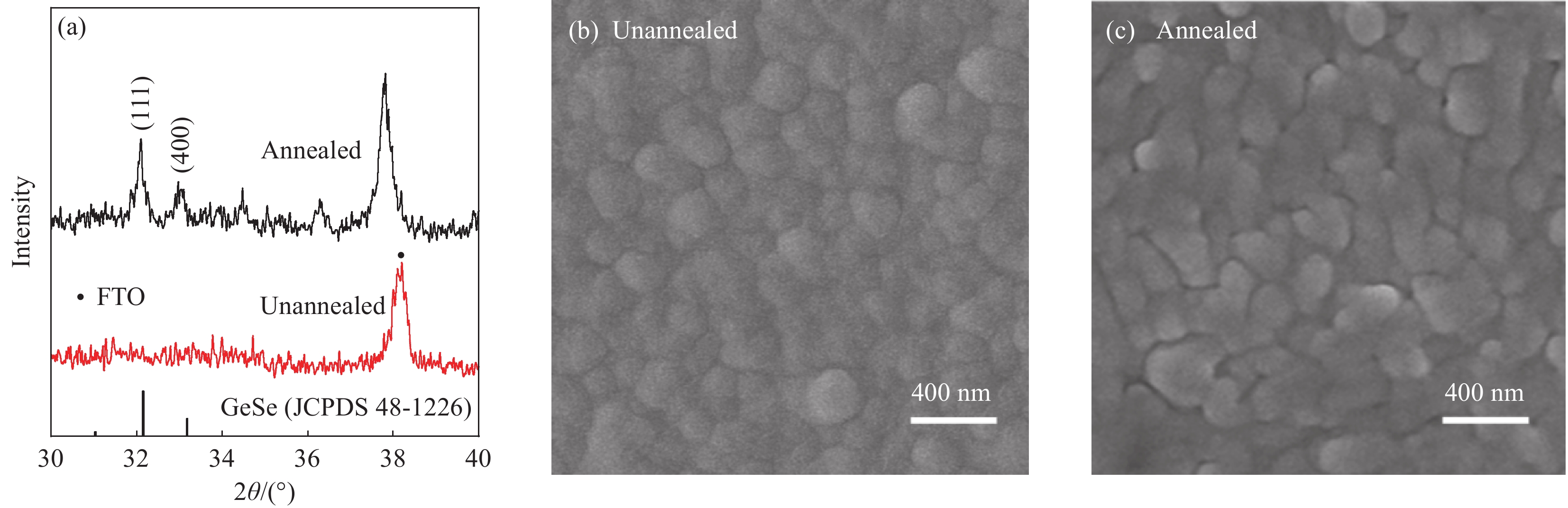
图 3 (a)未退火与退火GeSe薄膜的XRD图谱;未退火GeSe薄膜(b)和退火GeSe薄膜(c)的SEM图像
Figure 3. (a) XRD patterns of unannealed and annealed GeSe films; SEM images of unannealed GeSe film (b) and annealed GeSe film (c)

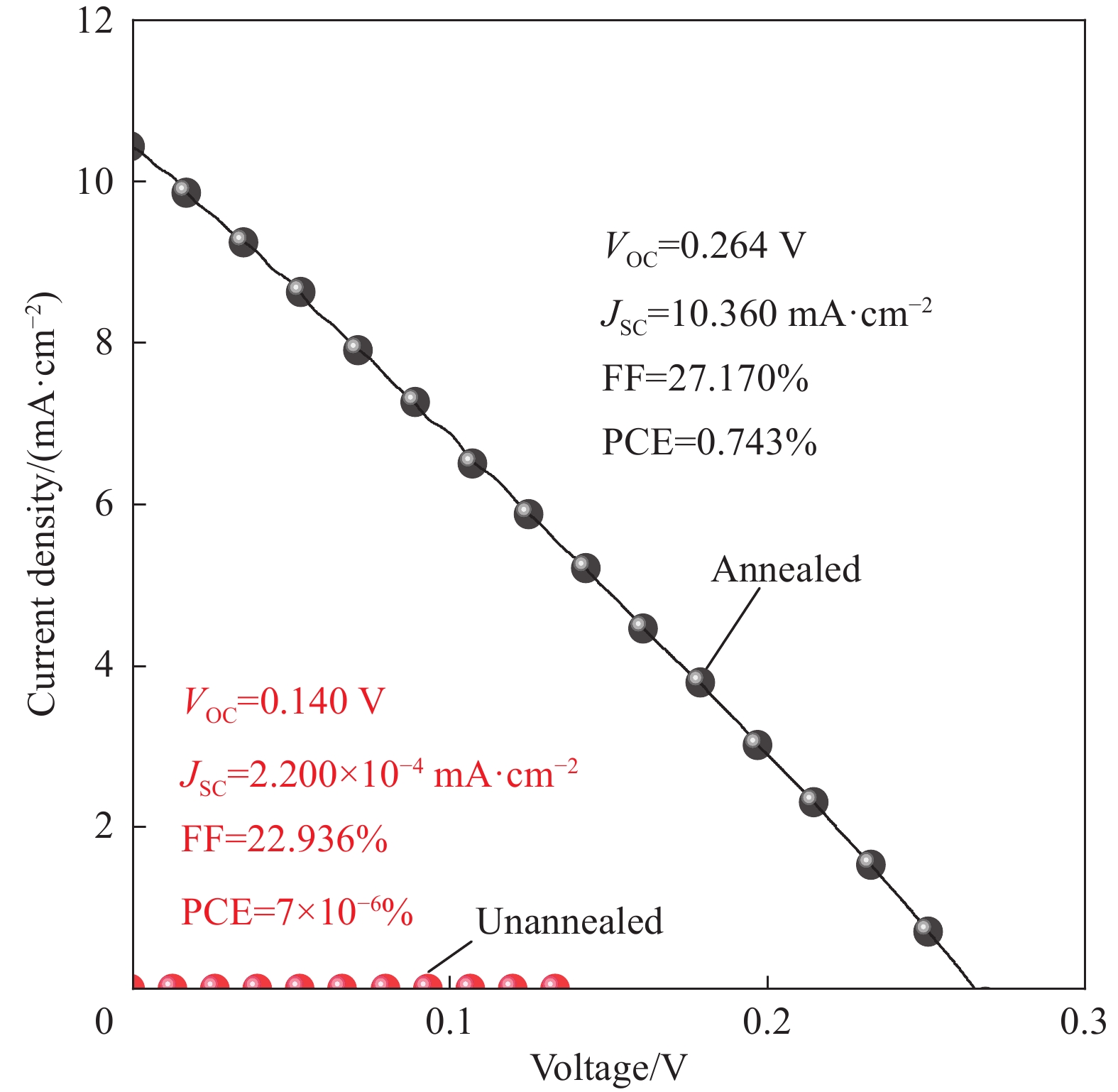
图 4 未退火与退火GeSe太阳能电池电流密度-电压(J-V)曲线
VOC—Open circuit voltage; JSC—Short circuit current density; FF—Filling factor; PCE—Photoelectric conversion efficiency
Figure 4. Current density-voltage (J-V) curves of unannealed and annealed GeSe solar cells

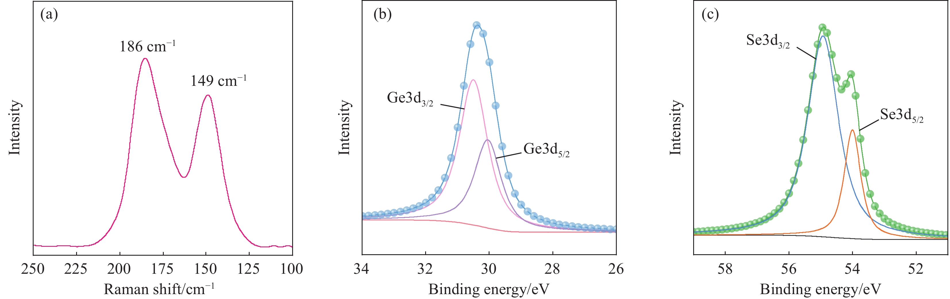
图 5 GeSe薄膜的拉曼图谱(a)和XPS图谱((b), (c))
Figure 5. Raman spectra (a) and XPS spectra ((b), (c)) of GeSe thin films

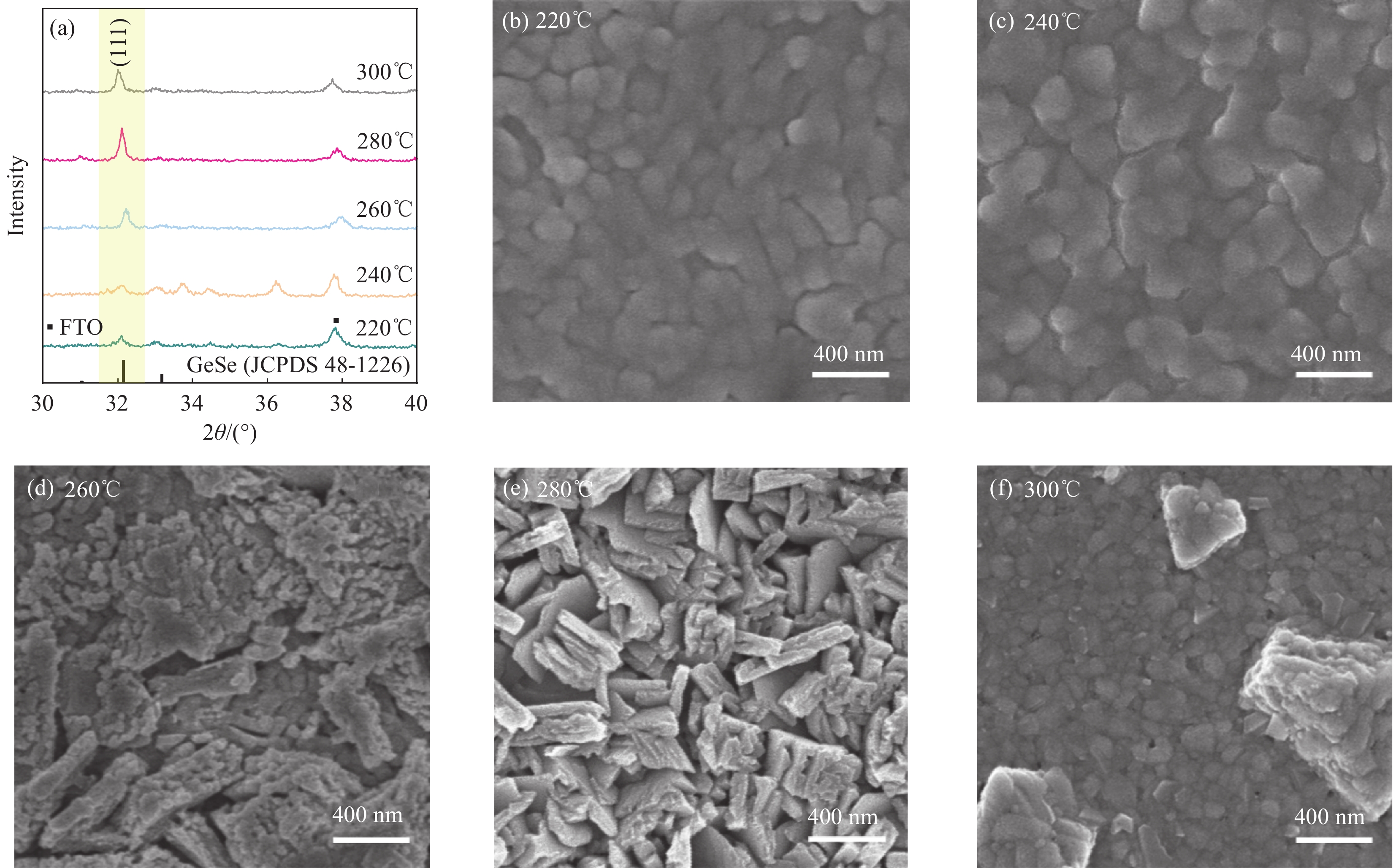
图 6 不同衬底温度下GeSe薄膜的XRD图谱(a)和SEM图像((b)~(f))
Figure 6. XRD patterns (a) and SEM images ((b)-(f)) of GeSe films under different substrate temperatures

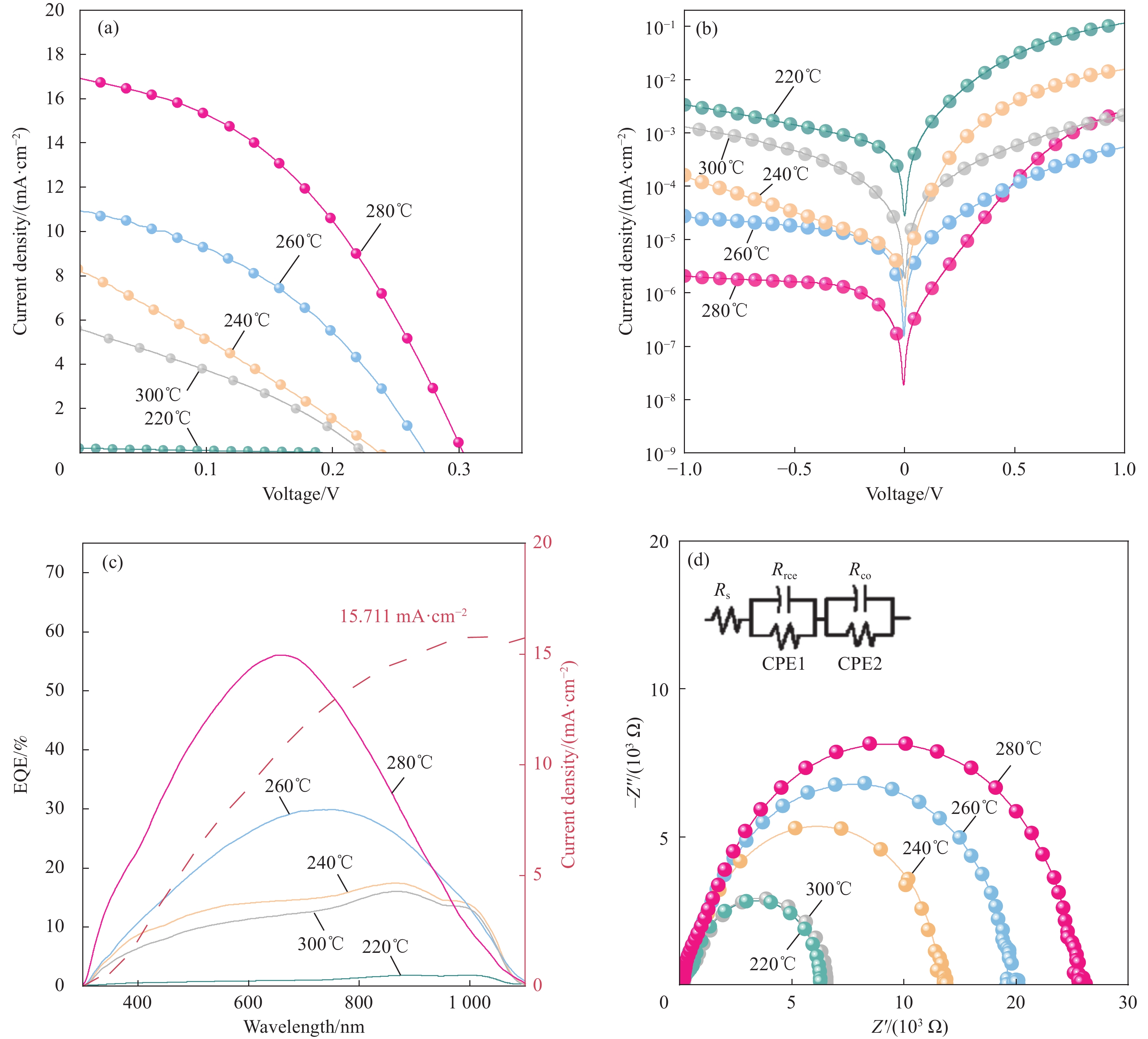
图 7 不同衬底温度下GeSe薄膜太阳能电池的光态J-V曲线(a)、暗态J-V曲线(b)、外部量子效率(EQE)曲线(c)和EIS曲线(d)
Rs—Series resistance; Rrec—Composite resistance; Rco—Contact resistance; Z'—The real part of the impedance; Z'' —The imaginary part of the impedance; CPE—Constant phase element
Figure 7. Light J-V curves (a), dark state J-V curves (b), external quantum efficiency (EQE) curves (c) and EIS impedance fitting curves (d) of GeSe thin film solar cells under different substrate temperatures

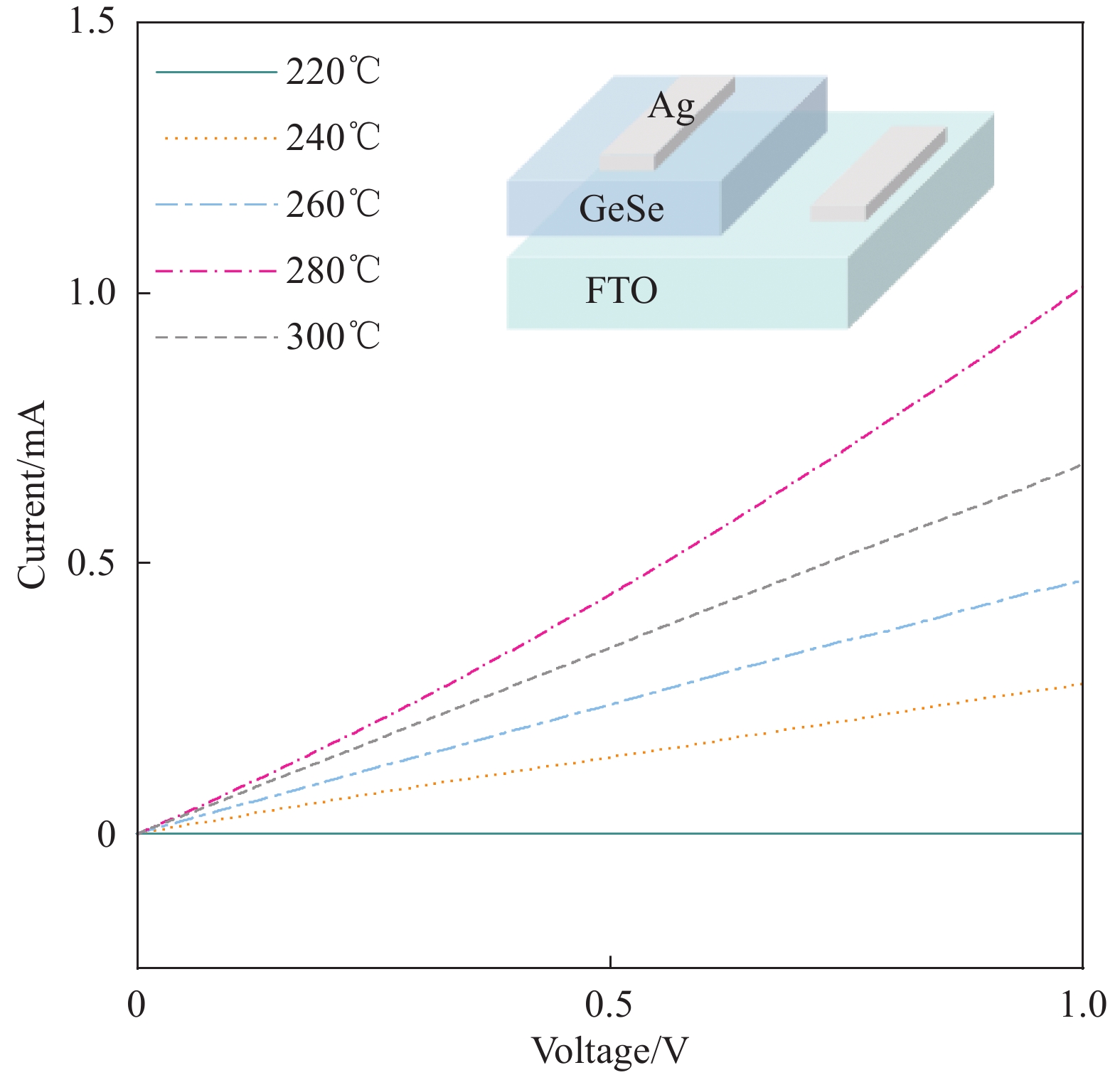
图 8 不同衬底温度下GeSe吸光层的电流-电压(I-V)曲线
Figure 8. Current-voltage (I-V) curves of GeSe absorbent layer at different substrate temperatures

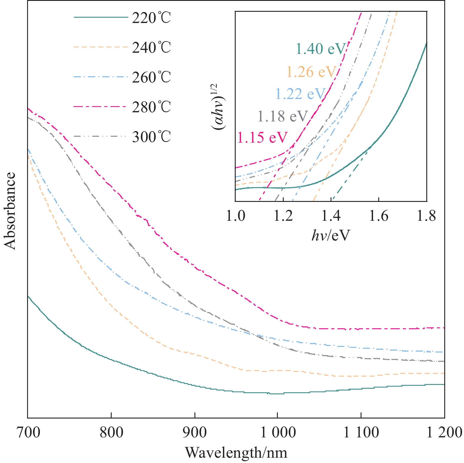
图 9 不同衬底温度下GeSe吸光层紫外-可见吸收光谱图(插图为对应GeSe薄膜的光学带隙图)
α—Absorption coefficient; hv—Photon energy
Figure 9. Ultraviolet-visible absorption spectra of the GeSe absorbent layer at different substrate temperatures (The illustration is the optical band gap diagram of the corresponding GeSe film)
表 1 不同衬底温度下GeSe薄膜太阳能电池的性能参数
Table 1. Performance parameters of GeSe thin film solar cells under different substrate temperatures
Substrate temperature/℃ VOC/V JSC/(mA·cm−2) FF/% PCE/% Grain size/nm τ/μs J0/(mA·cm−2) 220 0.228 0.211 22.571 0.011 18.855 34 3.123×10⁻⁵ 240 0.242 7.747 33.749 0.632 23.353 67 9.912×10⁻⁷ 260 0.269 10.892 40.137 1.178 48.079 89 8.091×10⁻⁷ 280 0.299 16.815 42.137 2.130 54.490 108 6.891×10⁻⁸ 300 0.225 5.583 31.906 0.401 40.867 42 1.328×10⁻⁶ Notes: τ—Specific conductance; J0—Reverse saturation current density.  下载: 导出CSV
表 2 EIS阻抗图中拟合阻抗参数
Table 2. Impedance parameters fitted in the EIS impedance diagram
Substrate temperature/℃ Rs/Ω Rrec/Ω Rco/Ω 220 147 6290 178 240 141 11500 167 260 135 14600 127 280 108 17420 60 300 140 6470 77
下载: 导出CSV
表 3 不同制备方法GeSe薄膜太阳能电池的特征参数
Table 3. Characteristic parameters of GeSe thin film solar cells prepared by different methods
下载: 导出CSV
-
[1] CAO Y, QU P, WANG C, et al. Epitaxial growth of vertically aligned antimony selenide nanorod arrays for heterostructure based self-powered photodetector[J]. Advanced Optical Materials, 2022, 10(19): 1-9. [2] ZHOU J, MENG D, YANG T, et al. Enhanced charge carrier transport via efficient grain conduction mode for Sb2Se3 solar cell applications[J]. Applied Surface Science, 2022, 591: 153169. doi: 10.1016/j.apsusc.2022.153169 [3] 樊娆, 王森阳, 梁成洋, 等. 不同浓度的 NiS2-FeS2/CNFs对电极对量子点敏化太阳能电池光伏性能的影响[J]. 复合材料学报, 2023, 40(12): 6681-6688.FAN Rao, WANG Senyang, LIANG Chengyang, et al. Effects of NiS2-FeS2/CNFs counter electrodes with different concentrations on the photovoltaic performance of quantum dot sensitized solar cells[J]. Acta Materiae Compositae Sinica, 2023, 40(12): 6681-6688(in Chinese). [4] WU J, LYU Y, WU H, et al. Stable GeSe LM solar cells employing non-toxic SnO2 as buffer layer[J]. Rare Metals, 2022, 4(9): 2992-2997. [5] YANG K, LI B, ZENG G. Effects of substrate temperature and SnO2 high resistive layer on Sb2Se3 thin film solar cells prepared by pulsed laser deposition[J]. Solar Energy Materials and Solar Cells, 2020, 208: 110381. [6] 孙北, 郑申申, 迟文晖, 等. Cu xO用于调控全无机碳基 CsPbI2Br 钙钛矿太阳能电池的界面性能[J]. 复合材料学报, 2023, 40(5): 2818-2826SUN Bei, ZHENG Shenshen, CHI Wenhui, et al. Improved interface performance of all inorganic carbon based CsPbI2Br perovskite solar cells using Cu xO[J]. Acta Materiae Compositae Sinica, 2023, 40(5): 2818-2826(in Chinese). [7] TIAN L, ZHANG W, HUANG Y, et al. Effects of annealing time on triple cation perovskite films and their solar cells[J]. ACS Applied Materials & Interfaces, 2020, 12(26): 29344-29356. [8] PATTINI F, RAMPINO S, MEZZADRI F, et al. Role of the substrates in the ribbon orientation of Sb2Se3 films grown by low-temperature pulsed electron deposition[J]. Solar Energy Materials and Solar Cells, 2020, 218: 110724. doi: 10.1016/j.solmat.2020.110724 [9] LIANG G, YU Z, XIE Z, et al. Optimizing the ratio of Sn4+ and Sn2+ in Cu2ZnSn(S, Se)4 precursor solution via air environment for highly efficient solar cells[J]. Solar RRL, 2021, 5(11): 2100574. doi: 10.1002/solr.202100574 [10] CHEN C, ZHAO Y, LU S, et al. Accelerated optimization of TiO2/Sb2Se3 thin film solar cells by high-throughput combinatorial approach[J]. Advanced Energy Materials, 2017, 7(20): 1700866. doi: 10.1002/aenm.201700866 [11] ZHOU J, ZHU J, HE W, et al. Selective preferred orientation for high-performance antimony selenide thin-film solar cells via substrate surface modulation[J]. Journal of Alloys and Compounds, 2023, 938: 168593. doi: 10.1016/j.jallcom.2022.168593 [12] FENG Z, LIU J, SU J, et al. Efficiency enhancement of a Sb2Se3 solar cell after adding a Si3N4 interface layer[J]. Materials Letters, 2020, 314: 131796. [13] MEDINA-MONTES M, MONTIEL-GONZALEZ Z, MATHEWS N, et al. The influence of film deposition temperature on the subsequent post-annealing and crystallization of sputtered Sb2S3 thin films[J]. Journal of Physics and Chemistry of Solids, 2017, 111: 182-189. doi: 10.1016/j.jpcs.2017.07.035 [14] MAO Y, WU X, CHEN H, et al. Controllable preparation of ultrathin GeSe nanosheets for infrared photodetection[J]. Infrared Physics & Technology, 2023, 132: 104736. [15] LI J, ZHAO Y, LI C, et al. Hydrazine hydrate-induced surface modification of CdS electron transport layer enables 10.30%-efficient Sb2(S, Se)3 planar solar cells[J]. Advanced Science, 2022, 9(25): 2202356. doi: 10.1002/advs.202202356 [16] ZHOU J, HE W, ZHU J, et al. Antimony selenide as a buffer layer for high-efficiency and highly crystalline germanium monoselenide thin-film solar cells[J]. Materials Letters, 2023, 333: 133584. doi: 10.1016/j.matlet.2022.133584 [17] LIU S, YANG Y, LI Z, et al. GeSe thin-film solar cells[J]. Materials Chemistry Frontiers, 2020, 4(3): 775-787. doi: 10.1039/C9QM00727J [18] SAIRAM A, SINGH Y, MAMTA, et al. Investigation of different configurations in gese solar cells for their performance improvement[J]. Journal of Nanomaterials, 2023, 2023: 1-14. [19] LYU T, LI X, YANG Q, et al. Stepwise Ge vacancy manipulation enhances the thermoelectric performance of cubic GeSe[J]. Chemical Engineering Journal, 2022, 442: 136332. doi: 10.1016/j.cej.2022.136332 [20] LYU X, WEI W, MU C, et al. Two-dimensional GeSe for high performance thin-film solar cells[J]. Journal of Materials Chemistry A, 2018, 6(12): 5032-5039. doi: 10.1039/C8TA00129D [21] CHENG K, GUO Y, HAN N, et al. Lateral heterostructures of monolayer group-IV monochalcogenides: Band alignment and electronic properties[J]. Journal of Materials Chemistry C, 2017, 5(15): 3788-3795. doi: 10.1039/C7TC00595D [22] HUO G, WANG D, ALI R, et al. CH3NH3PbI3/GeSe bilayer heterojunction solar cell with high performance[J]. Solar Energy, 2018, 159: 142-148. doi: 10.1016/j.solener.2017.10.074 [23] XUE D, LIU S, DAI C, et al. GeSe thin-film solar cells fabricated by self-regulated rapid thermal sublimation[J]. Journal of the American Chemical Society, 2017, 139(2): 958-965. doi: 10.1021/jacs.6b11705 [24] CHEN B, CHEN G, WANG W, et al. Magnetron sputtering deposition of GeSe thin films for solar cells[J]. Solar Energy, 2018, 176: 98-103. doi: 10.1016/j.solener.2018.10.030 [25] ZI W, MU F, LU X, et al. Post-annealing treatment of a-GeSe thin films for photovoltaic application[J]. Solar Energy, 2020, 199: 837-843. doi: 10.1016/j.solener.2020.02.086 [26] LIU S, DAI C, MIN Y, et al. An antibonding valence band maximum enables defect-tolerant and stable GeSe photovoltaics[J]. Nature Communication, 2021, 12(1): 670. doi: 10.1038/s41467-021-20955-5 [27] SONG J, ZHENG E, WANG X, et al. Low-temperature-processed ZnO-SnO2 nanocomposite for efficient planar perovskite solar cells[J]. Solar Energy Materials and Solar Cells, 2016, 144: 623-630. doi: 10.1016/j.solmat.2015.09.054 [28] YANG F, LI X, REN Z, et al. The NC-Si films with controlled crystal structure and electrical conductivity via the re-crystallization approach[J]. Journal of Non-crystalline Solids, 2013, 359: 40-45. doi: 10.1016/j.jnoncrysol.2012.10.006 [29] LIU S, ZONG L, JIN W, et al. Boosting the efficiency of GeSe solar cells by low-temperature treatment of p-n junction[J]. Science China Materials, 2021, 64(9): 2118-2126. doi: 10.1007/s40843-020-1617-x -

 下载:
下载:


 点击查看大图

计量
- 文章访问数: 258
- HTML全文浏览量: 161
- PDF下载量: 6
- 被引次数: 0
